Materials for
Semiconductor
Photo Process
Semiconductor
Application Materials
The fine chemical materials used in the core process of semiconductor manufacturing,
the photo process, are based on synthesis and purification technologies.
Main Products
Materials for Photo Process
Photoresist is a material that responds sensitively to specific wavelengths of light and changes its properties. It is a photosensitive material used in the core process of semiconductor pattern formation (photolithography), consisting of polymers, Photo Acid Generator (PAG), and additives.
-
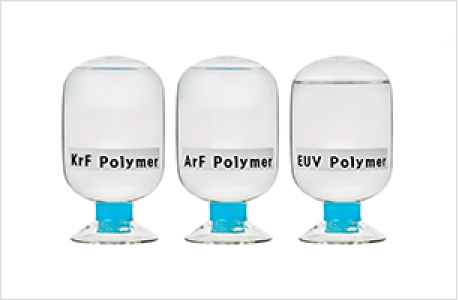
 Polymer for PR
The key chemical substance that determines characteristics
-
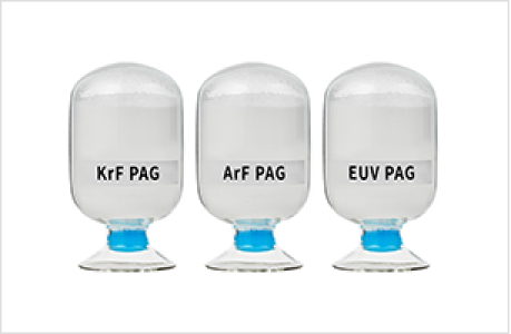
 PAG for PR
(Photo Acid Generator)When it absorbs light, acid is generated, which acts as a catalyst to modify the polymer structure and form a pattern.
-
 Monomer for PR
Starting substance of polymer
-
 Additive for PR
Substance that plays a supporting role in the performance of Photo Resist.
A material that complements the thin photoresist, which forms micro patterns, forms
a protective layer on the photoresist or helps to prevent the bending of light to aid in the formation of well-defined patterns.
-
 Polymer for BARC
As a reflection-resistant layer coated on the bottom of PR, it is a substance that helps to suppress problems caused by light reflected onto the substrate during the photolithography process, allowing for consistent patterning.
-
 Polymer/Monomer for SOH
Plays a role as a supporting layer to prevent the collapse of the photoresist during the etching process as the pattern becomes finer.


